PART 1: INTRODUCTION
Page: 3-3 (1)
Author: Terence K.S. Wong
DOI: 10.2174/978160805359911201010003
PDF Price: $15
Introduction to Strain Metrology for Semiconductors
Page: 4-14 (11)
Author: Terence K.S. Wong
DOI: 10.2174/978160805359911201010004
PDF Price: $15
Abstract
Two conventional strain measurement methods, namely the strain gauge and the Moire technique are first discussed. The origin of interest in strain effects in semiconductors is introduced in a chronological sequence beginning with stressed induced defects near isolation structures and the present intentional use of strain in the channel of field effect transistors as a performance booster. The need and the lack of precise strain measurement methods at the submicron and nanoscale are emphasized. Strain measurement for microelectromechanical device materials is also discussed.
Strain, Stress and Semiconductor Properties
Page: 15-26 (12)
Author: Terence K.S. Wong
DOI: 10.2174/978160805359911201010015
PDF Price: $15
Abstract
This tutorial chapter provides a synopsis of the theoretical concepts needed for understanding subsequent chapters. The concepts of engineering strain, true strain, Eulerian strain and in particular, the tensor nature of strain are first introduced. The components of the stress tensor which give rise to strain are next discussed. The three main elastic properties of solids namely: Young’s modulus, shear modulus and Poisson’s ratio are defined. The piezoresistance effect introduced in the first chapter is discussed quantitatively. This is followed by two topics on the optical properties of semiconductors, the Kramers-Kronig relation and the optical joint density of states used in optical strain metrology.
PART 2: OPTICAL STRAIN METROLOGY
Page: 27-27 (1)
Author: Terence K.S. Wong
DOI: 10.2174/978160805359911201010027
PDF Price: $15
Abstract
In this part, we describe three strain metrology techniques that make use of the interaction of light with a sample to measure strain. The optical interactions are: (i) reflection, (ii) polarization change and (iii) inelastic scattering. Although the interactions used are different for each technique, they share a common principle that they are based on the so-called morphic effects of semiconductors. The morphic effects are basically perturbation effects by external influences such as stress or pressure on the crystal structure and the band structure of a semiconductor. By measuring the changes in the band structure, it is possible for instance to infer the magnitude of the strain that causes the perturbation.
All three techniques make use of visible and ultraviolet light and are non-destructive and non-invasive. They therefore involve little or no sample preparation and are well suited to the routine process monitoring of strained semiconductor substrates such as strained silicon and strained silicon on insulator. However, the techniques are mainly ex situ and with the exception of the Raman spectroscopy technique cannot be applied to individual transistors on wafer. The tip-enhanced Raman technique with higher spatial resolution is at present under development and is not yet ready for manufacturing.
Variable Angle Spectroscopic Ellipsometry
Page: 28-37 (10)
Author: Terence K.S. Wong
DOI: 10.2174/978160805359911201010028
PDF Price: $15
Abstract
Strain measurement based on reflection of polarized light from the strained semiconductor sample is explained in this chapter. Spectroscopic ellipsometry is usually applied for thickness measurement of thin films of materials with known optical functions. In this approach, the optical functions are found with the layer thickness determined from additional separate measurements. From the fitted optical function spectra, the shift in energy of the critical point can be determined mathematically and using the deformation potential, the strain can be obtained.
Photoreflectance Method
Page: 38-49 (12)
Author: Terence K.S. Wong
DOI: 10.2174/978160805359911201010038
PDF Price: $15
Abstract
A modulated spectroscopy method called photoreflectance is described. The technique involves using an incident beam and a coincident modulating beam usually from a diode laser. The former results in a reflectance signal while the latter gives a modulated reflectance signal. By fitting the spectrum of the normalized modulated reflectance with a third order derivative of the dielectric function, the critical point energies can be determined with high accuracy. Two photoreflectance spectroscopy instruments with high throughput are discussed. The use of these instruments is illustrated by examples from biaxially stressed silicon on insulator substrates and thin film photovoltaic devices. A recent method to suppress spurious modulated light from entering the photodetector is also briefly discussed.
Micro-Raman Spectroscopy
Page: 50-58 (9)
Author: Terence K.S. Wong
DOI: 10.2174/978160805359911201010050
PDF Price: $15
Abstract
The use of inelastic scattering of laser light or Raman scattering to measure strain with micron scale spatial resolution is reviewed in this chapter. The principle of Raman scattering is discussed first and is followed by the effect of strain on the frequency shift of Raman scattered light. The experimental setup for performing Raman scattering measurements and the needed experimental precautions are given in detail. The method is illustrated by examples from strained silicon, polycrystalline silicon and strain fields near device isolation structures in crystalline silicon.
PART 3: ELECTRON BEAM STRAIN METROLOGY
Page: 59-59 (1)
Author: Terence K.S. Wong
DOI: 10.2174/978160805359911201010059
PDF Price: $15
Abstract
In this part, we describe three methods of strain metrology that are based upon the use of electron microscopes. Either a finely focused electron beam in a scanning electron microscope (SEM) or a collimated electron beam in a transmission electron microscope (TEM) can be used to obtain strain information from a semiconductor sample. Unlike the optical methods in part 2, all three methods are suitable for probing device structures because electron beam techniques have much higher spatial resolution and the researcher can select the area of interest within the sample. The cathodoluminescence method of chapter 6 is based on the effect of strain upon the bandgap of a semiconductor. From the standpoint of principle, it is similar to the methods in chapters 3 to 5.
The other two methods in this part make use of the wave property of the electron. The electron diffraction methods of chapter 7 discuss two recent techniques: nanodiffraction and convergent beam electron diffraction. Both techniques had been applied to probe the strain distribution within strained silicon transistors. The electron holographic Moire method of chapter 8 is a very new and promising method. It makes use of the interference of two coherent electron beams from the same electron source in a TEM to generate an electron hologram. Unlike conventional holograms, one beam passes through a strained region of the sample and the other beam passes through an unstrained substrate region of the sample. Strain information is then extracted from the phase image derived from the electron hologram by the geometrical phase analysis method developed originally for high resolution TEM.
Cathodoluminescence Method
Page: 60-69 (10)
Author: Terence K.S. Wong
DOI: 10.2174/978160805359911201010060
PDF Price: $15
Abstract
A strain characterization method with nanoscale spatial resolution called cathodoluminescence is explained. The method involves the use of a small electron probe with high energy. The energy loss by the primary electrons results in the emission of light which are collected by reflective optics and detected by a spectrometer. By measuring the cathodoluminescence spectrum during scanning, a spatial map of the stress distribution can be deduced. This is because stress affects the peak of the emission spectrum from the sample via the piezospectroscopic effect. By monitoring the peak shift, the strain can be deduced from the piezospectroscopic coefficients. This method is especially useful for ceramic materials such as oxides and glasses for which the Raman effect is extremely weak. However, stress distribution in epitaxial III-nitride semiconductors had also been studied.
Nano-Beam Diffraction and Convergent Beam Electron Diffraction
Page: 70-79 (10)
Author: Terence K.S. Wong
DOI: 10.2174/978160805359911201010070
PDF Price: $15
Abstract
Two electron crystallographic techniques capable of measuring strain in nanoscale regions of a device sample are discussed. Both require the use of an analytical TEM. In nano-beam diffraction, a small collimated beam is diffracted by a crystalline sample and by measuring the distances between diffraction spots, the lattice spacing in the strained region can be found. This together with a separate measurement at the unstrained region will allow the strain to be characterized. The second method uses a convergent electron beam and involves measuring the shifts in the higher order Laue zone lines which are more sensitive to strain. In order to access these lines in the analytical TEM, sample tilting is required. This however limits the spatial resolution of the convergent beam electron diffraction technique to about 50nm.
Dark-Field Electron Holographic Moire Method
Page: 80-89 (10)
Author: Terence K.S. Wong
DOI: 10.2174/978160805359911201010080
PDF Price: $15
Abstract
A strain measurement method based on the quantum interference of coherent electron waves scattered from adjacent strained and unstrained regions of a device is discussed. The method is related to the off axis electron holography technique and is carried out in analytical TEMs equipped with an ultra-stable electron source, Lorentz lens, electron biprism and quantitative HREM software. The hologram obtained by interference of two diffracted beams from a set of lattice planes is analyzed by Fourier transformation to obtain the phase image. The geometric phase analysis used previously for strain mapping in HREM images is performed on the phase image to give the strain with high spatial resolution. This resolution is determined by the hologram fringe spacing. Moreover, all components of the strain tensor can be obtained if more than one diffracted beam is used. The method has been demonstrated for strained silicon device structures and silicon-silicon germanium epitaxial layers.
PART 4: EMERGING STRAIN METROLOGY
Page: 90-90 (1)
Author: Terence K.S. Wong
DOI: 10.2174/978160805359911201010090
PDF Price: $15
Abstract
In this final part, we survey three emerging cross-disciplinary strain metrology methods. These methods share a common feature that they are ‘in situ’ methods. The strain measurement is carried out within or with the assistance of a microscope or a synchrotron light source. The tip-enhanced Raman spectroscopy method (chapter 9) used the same principle as that described in chapter 5 for thin films. However, the spatial resolution of the Raman spectroscopy is enhanced by using the surface plasmon resonance of a metallic atomic force microscope tip. This near field interaction increases the Raman scattering from a small region beneath the metallic probe but it does not change the far field Raman signal which is still present. This technique is now of great interest to the microelectronics industry and may eventually find application for characterizing strained semiconductor devices. The next method atomic force microscopy digital image correlation (chapter 10) is used mainly by mechanical engineers for MEMS devices. It is an image correlation method for finding the strain distribution in a sample under deformation. The sample is strained and imaged by the atomic force microscope probe at the same time. The last method in this volume is X-ray micro/nanodiffraction. This technique requires a high intensity X-ray beam. As a result, this method requires access to high brilliance synchrotron sources. At present, it is difficult to see how this type of method can be of routine use to the semiconductor industry.
Tip-Enhanced Raman Spectroscopy
Page: 91-101 (11)
Author: Terence K.S. Wong
DOI: 10.2174/978160805359911201010091
PDF Price: $15
Abstract
A strain measurement method based on nanophotonics is described. In this technique, a noble metal probe or nanoparticle film is used to enhance the probability of Raman scattering by using the surface plasmon resonance effect. An incident laser with a wavelength tuned to the surface plasmon resonance excites surface plasmons in a metal nanoparticle. As a result, the electromagnetic field near the probe is enhanced. The region in which Raman scattering is enhanced is in the nanoscale and the spatial resolution of the Raman microprobe is thereby extended. The method requires a scanning probe microscope to be coupled to a confocal Raman microscope and spectrometer. The development of high contrast tip enhanced Raman spectroscopy and tip preparation techniques are discussed.
Atomic Force Microscopy Digital Image Correlation Method
Page: 102-111 (10)
Author: Terence K.S. Wong
DOI: 10.2174/978160805359911201010102
PDF Price: $15
Abstract
An in situ method of strain characterization based on image analysis of atomic force microscope images is presented. The sample topographic image is measured before and after deformation using an atomic force microscope with closed loop feedback control of position. By using a mapping function for each point in the image and performing a correlation using the height data, the displacement, strain and strain gradient can be deduced. The digital image correlation algorithm is most suitable for microelectromechanical materials and devices.
Synchrotron X-ray Micro/Nanodiffraction Methods
Page: 112-125 (14)
Author: Terence K.S. Wong
DOI: 10.2174/978160805359911201010112
PDF Price: $15
Abstract
Several X-ray diffraction methods using synchrotron sources are discussed in this chapter. For epitaxial semiconductor samples, high resolution double axis and reciprocal space mapping methods are applicable and measurement time can be reduced by the use of synchrotron radiation. The lattice strain can be deduced directly from the measured inter-planar spacing using Bragg’s law without modeling. Polycrystalline samples such as metal films are measured by the sin2Ψand sin2Ψmethods. Interconnects with widths of the order of one micron can be mapped at this spatial resolution by a scanning X-ray microdiffraction technique. This method does not involve sample rotation by a goniometer. The strain tensor is deduced from an analysis of the von Laue diffraction image and comparison with a structural model of the sample. A high flux density polychromatic X-ray beam is essential for this method.
Conclusion and Outlook
Page: 126-128 (3)
Author: Terence K.S. Wong
DOI: 10.2174/978160805359911201010126
PDF Price: $15
Abstract
Some general remarks are given for all the strain characterization methods discussed in previous chapters. The methods can be categorized into those where a strain related material property must be known and those that do not require such a priori knowledge. The different available methods are briefly compared with each other in terms of the strain resolution, spatial resolution, throughput and accessibility. The future application of semiconductor strain characterization techniques in electrical energy storage devices is suggested and a recent development of strain characterization by electron backscattering from epitaxial layers is highlighted.
Appendix 1
Page: 129-131 (3)
Author: Terence K.S. Wong
DOI: 10.2174/978160805359911201010129
PDF Price: $15
Introduction
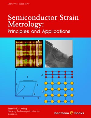
This book surveys the major and newly developed techniques for semiconductor strain metrology. Semiconductor strain metrology has emerged in recent years as a topic of great interest to researchers involved in thin film and nanoscale device characterization. This e-book employs a tutorial approach to explain the principles and applications of each technique specifically tailored for graduate students and postdoctoral researchers. Selected topics include optical, electron beam, ion beam and synchrotron x-ray techniques. Unlike earlier references, this e-book specifically discusses strain metrology as applied to semiconductor devices with both depth and focus.


